SiC and AlN submounts · Hermetic packages
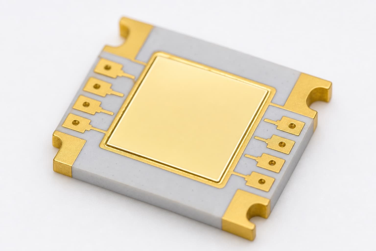
Laser diode submounts and hermetic packages.
Single-crystal SiC (350–400 W/m·K) and polycrystalline AlN (170–210 W/m·K). Evaluation samples in 2–4 weeks. TO headers, 14-pin butterfly, and cavity outlines quoted from the same engineering contact.
Products
Submounts spread heat at the die; hermetic packages seal and route the optical stack. Browse both from one engineering partner.
Thermal submounts
Die-level spreading by application — laser, datacom, and power/RF. Samples ship in 2–4 weeks.
Submount catalogRFQHermetic metal packages
TO headers, butterfly, cavity housings, and mount hardware — 50+ SKUs with engineering quotes.
Browse packagesSoonActive thermal
TEC modules and cold plates — qualification in progress.
Learn moreThermal submounts
By application · evaluation samples · 2–4 week lead time
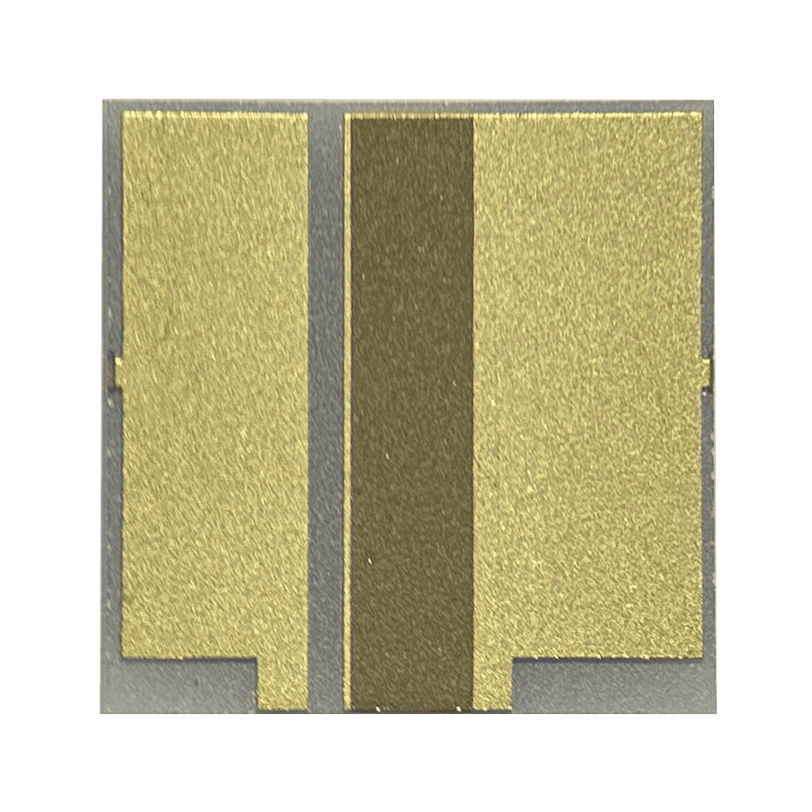
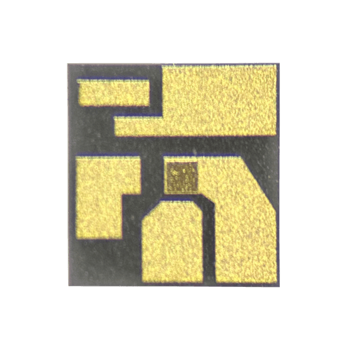
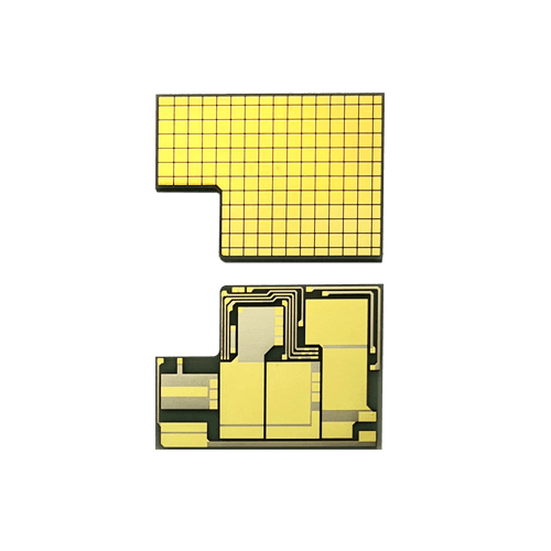
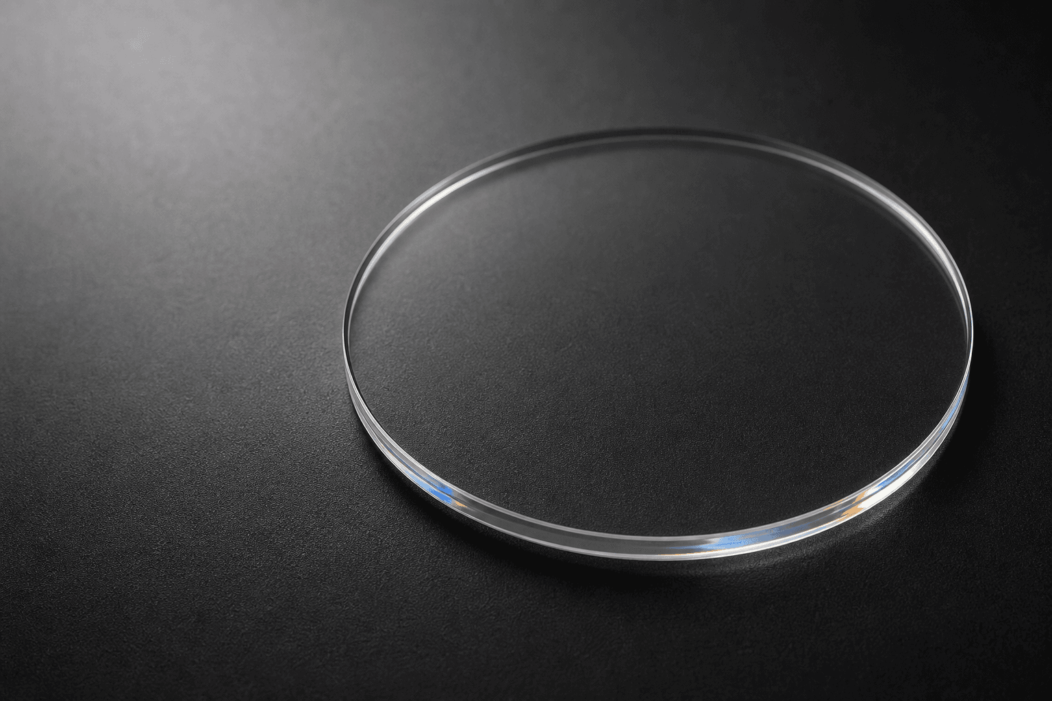
Hermetic metal packages
Engineering quote · ISO-certified supply · 50+ outlines
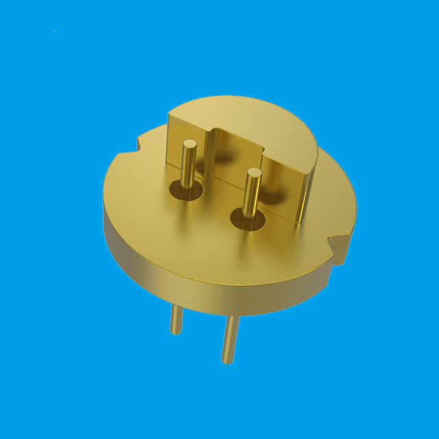
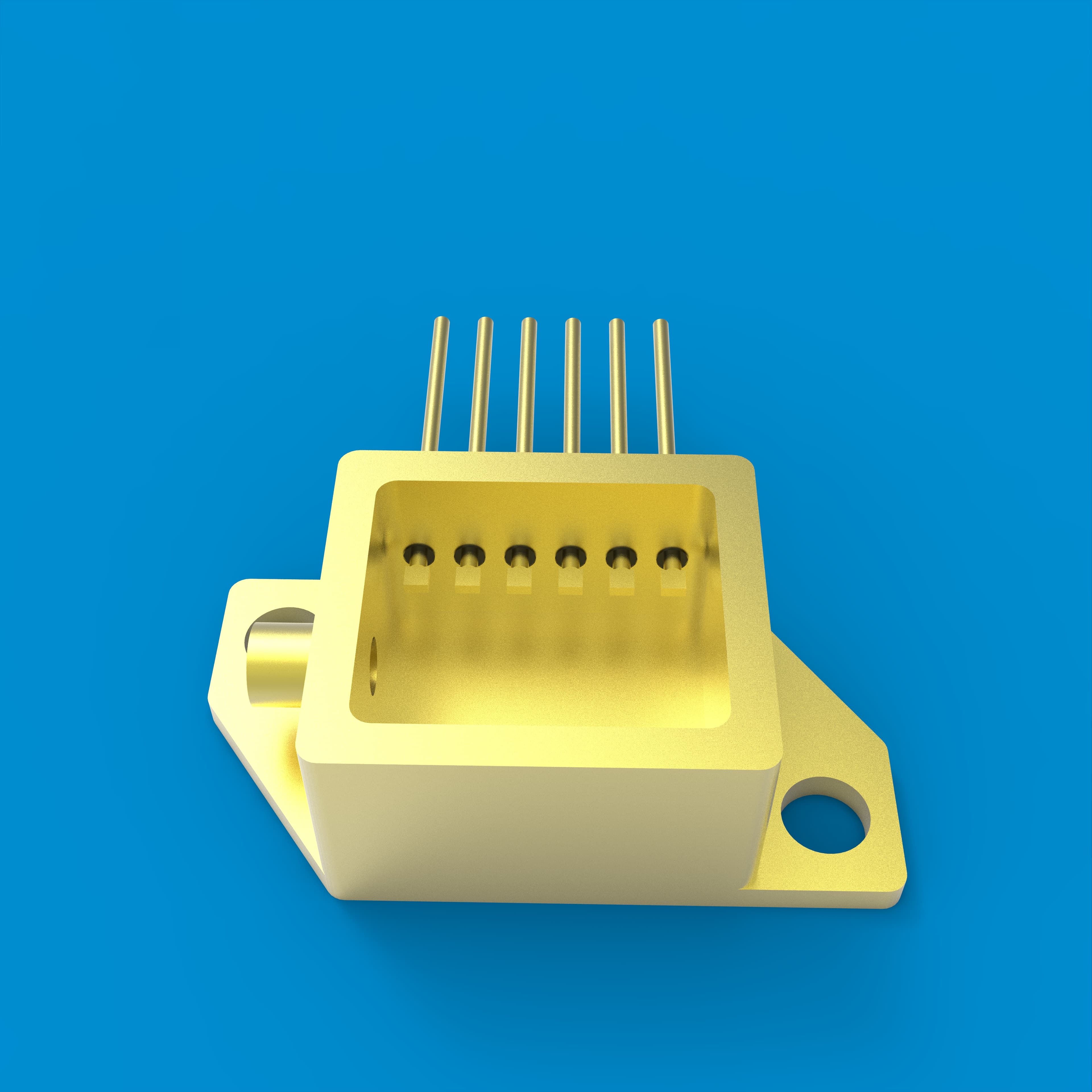
Custom submounts and package drawings — free DFM review or info@ferralink.com
Key outcomes
≤1×10⁻³ Pa·cm³/s
Hermetic packages tested to the tightest leak rate standards.
Every hermetic package meets ≤1.0×10⁻³ Pa·cm³/s leak rate, ≥500V AC dielectric withstanding, and ≥10,000 MΩ insulation resistance — qualified for −65°C to +150°C operating environments.
Learn more →Unique350 W/m·K
Single-crystal SiC — the highest thermal conductivity available in a ceramic submount.
Without polycrystalline grain boundaries, phonon transport is unimpeded. FerraLink supplies qualified single-crystal SiC submounts with documented thermal performance.
Learn more →Precision170 W/m·K
Polycrystalline ALN — best CTE match for InP and GaAs laser diodes.
Grain boundaries limit conductivity to 170–210 W/m·K — still 6–8× better than alumina. The right choice when CTE matching and cost matter more than absolute thermal performance.
Learn more →Speed2–4 weeks
Typical first-sample turnaround — so your program stays on schedule.
From design review to first article in weeks, not months. Responsive engineering support means you iterate quickly from prototype to production without sacrificing quality.
Learn more →Submount Advisor
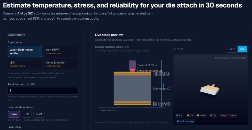
Free · ~30 secValidate your die attach before you freeze the BOM
Enter chip size and peak power once. Get an indicative thermal profile, stress screening, failure-mode hints, and a customized part number — not a pick from a fixed size chart.
- Check junction temperature & thermal margin3D steady-state model on your die size, power, and submount geometry — see where heat accumulates.
- Screen failure mechanisms earlyIndicative AuSn fatigue, die stress, and warpage bands before you commit to a BOM.
- Any footprint — not a fixed catalog gridEnter your dimensions; we generate a part number, stack layout, and spec PDF in real time.
- Quote-ready outputDownload the spec sheet, request samples, or send the configuration straight to FerraLink.
Work email unlocks the tool, your part number, and spec PDF export. Always free — we follow up only if you request samples or a quote.
Order evaluation samples
10-piece standard sample boxes — evaluate FerraLink quality directly in your lab before committing to production. Ships within 2–4 weeks with full material documentation.
Need a hermetic package quote instead? Request package quote — TO headers, butterfly, and cavity outlines.
Place your order
Order summary
← Select a sample box
We confirm and send a payment link within 1 business day.
Engineering services
FerraLink is not only a parts supplier — we help you select materials, freeze stackups, and move from sample evaluation to custom production.
DFM review
Send your drawing — feasibility, lead time, MOQ, and risk flags within 2 business days.
Start DFM review →Submount co-design
Chip + system review → submount geometry, metallization, and package stackup with part numbers.
Book walkthrough →Prototype → production
Standard samples first, then custom qualification at ~2,000 pc MOQ, then production release.
See full path →How we work
Small volume means standard samples only. Custom submounts typically require a 2,000 pc MOQ — we respond to RFQs within 2 business days.
Standard samples
- ALN box $250 · SiC box $500
- Catalog samples from $25 / $50
- Lead time 2–4 weeks
Custom production
- Custom size, pads, metallization
- DXF, Gerber, STEP accepted
- Lead time quoted after DFM
| Order type | Typical lead time |
|---|---|
| Standard sample box | 2–4 weeks |
| Catalog sample | 2–4 weeks |
| Custom geometry | Quoted per project |
| Production repeat | Quoted per PO |
Industries we serve
FerraLink components are qualified and in use across demanding applications where thermal performance, hermeticity, and precision matter.
TO18/46/56, butterfly packages, 25G/100G TOSA/ROSA, optical transceivers
Hermetic cavity packages, HTCC ceramics, high-reliability ALN submounts
High-power TO headers, SiC submounts, AuSn solder preforms, lensed caps
Hermetic SMT packages, sapphire optical windows, sensor housings
RGB laser packages, cavity packages, ALN substrates with CTE-matched metallization
DBC/AMB substrates, HTCC packages, current capacity >50 A, up to mm-wave frequencies
SiC and ALN DBC/AMB substrates for EV, traction, and industrial power modules
High-density thick-film substrates, solid metal vias, integrated resistors
Why FerraLink
Engineering teams have three options for submounts and hermetic packaging. Here is an honest comparison.
Why not buy direct from a manufacturer?
Direct relationships with overseas manufacturers require MOQs, long lead times, and managing quality across language and timezone barriers. One supplier change can stall your program for months.
FerraLink qualifies manufacturing partners per program, holds standard catalog paths, and gives you one global engineering point of accountability — without the overhead of managing factory relationships yourself.
Why not use a general distributor?
General distributors fill orders — they don't help you select substrate material, troubleshoot hermetic seal failures, or adapt a package design to your thermal requirements. You get catalog numbers, not engineering guidance.
FerraLink engineers speak the language of thermal design, hermeticity, and optical alignment. We help you select the right substrate, metallization, and package before you place an order — and stay accountable through qualification.
Why FerraLink for SiC?
SiC submounts deliver 350–400 W/m·K — the highest thermal conductivity in any practical ceramic substrate. Catalog distributors rarely stock them, and qualification documentation is often inconsistent across sources.
FerraLink supplies qualified single-crystal SiC submounts with standard catalog sizes, custom dimensions and metallization, and evaluation samples in 2–4 weeks — backed by material documentation on every shipment.
Technology
FerraLink partners deliver precision ceramics and hermetic packaging using the same fabrication technologies found in defense, telecom, and aerospace supply chains.
Performance benefits
Fine-line patterning
DPC process achieves minimum line/space of 50 µm on ALN and SiC — enabling dense photonic and RF circuit layouts.
High current capacity
Thick plated copper metallization on ceramic carriers handles >50 A continuously — suitable for power modules and driver circuits.
Hermetic integrity
All hermetic packages tested to ≤1.0×10⁻³ Pa·cm³/s leak rate and ≥500 V AC dielectric withstanding voltage.
Qualified environments
Packages qualified through 1000+ thermal cycles per MIL-STD-810 — ready for defense, aerospace, and industrial deployment.
Substrate material comparison
| Property | Diamond | SiC | ALN | Al₂O₃ (Alumina) |
|---|---|---|---|---|
| Crystal structure | CVD polycrystalline | Single crystal | Polycrystalline | Polycrystalline |
| Thermal conductivity | 1,500–2,200 W/m·K | 350–400 W/m·K | 170–210 W/m·K | 26–30 W/m·K |
| CTE (ppm/°C) | 1.0–1.5 | 3.7–4.3 | 4.3–4.6 | 6.7–8.1 |
| Availability | Pre-release | In production | In production | Industry standard |
| Device compatibility | Extreme power density | GaN, Si, lidar | Si, GaAs, InP | GaAs-based (general use) |
| Key benefit | Highest spreading available | Best production ceramic κ | Best CTE for InP/GaAs | Low cost |
| Typical application | Multi-kW bars, RF hotspots | Power electronics, lidar | Laser diode, RF, optical | General substrates |
Material verification — SEM & EDS
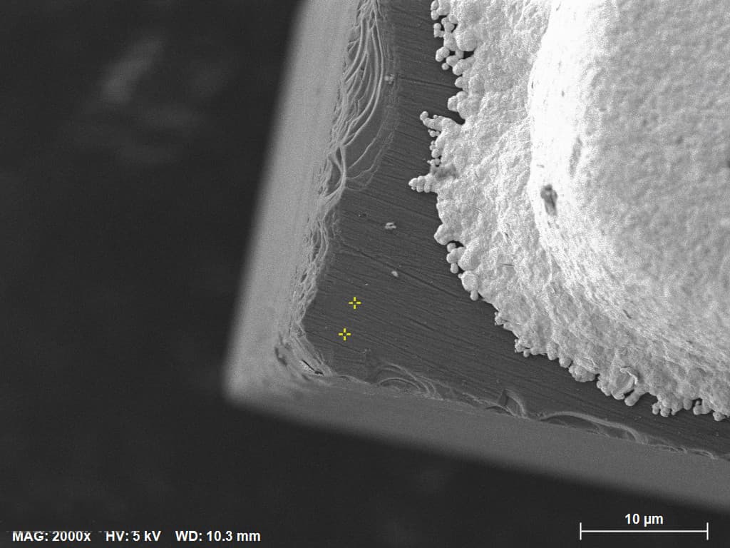
The thermal performance difference between SiC and ALN starts at the microstructure level. Single-crystal SiC conducts heat with minimal phonon scattering, while polycrystalline ALN — though still far superior to alumina — loses conductivity at every grain boundary.
SiC (single crystal)
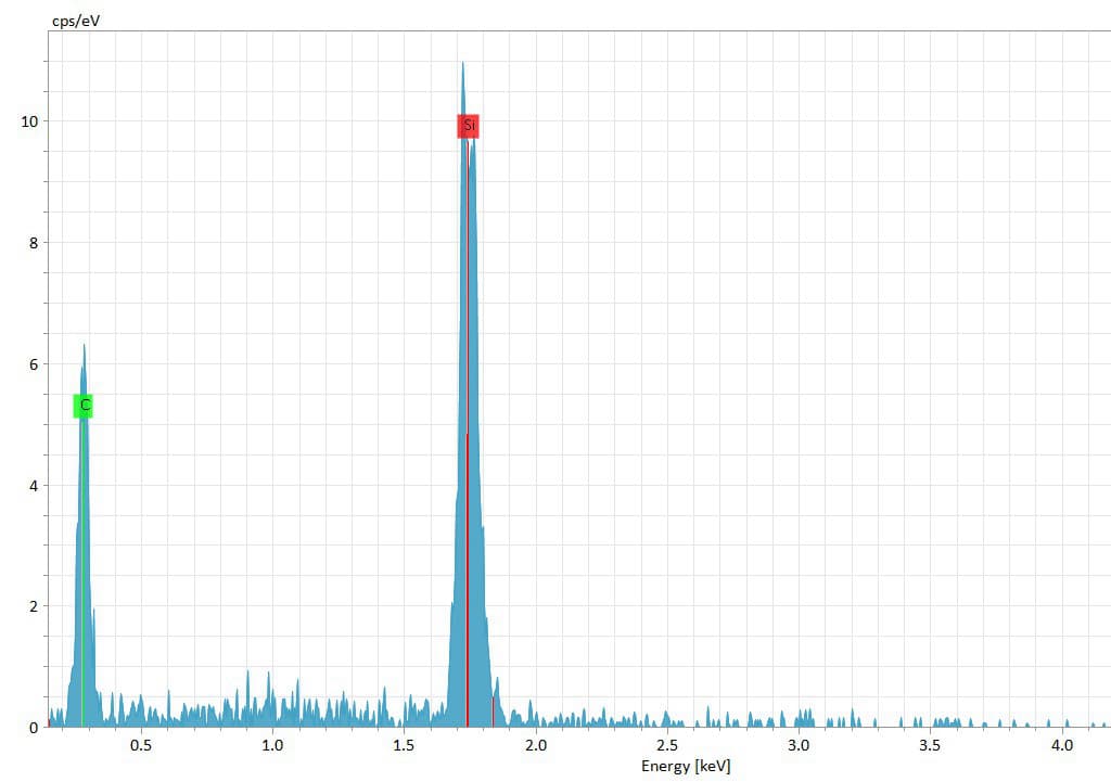
FerraLink SiC submounts use single-crystal silicon carbide. Without grain-boundary phonon scattering, thermal conductivity reaches 350–400 W/m·K — the highest of any practical ceramic substrate available to packaging engineers.
ALN (polycrystalline)
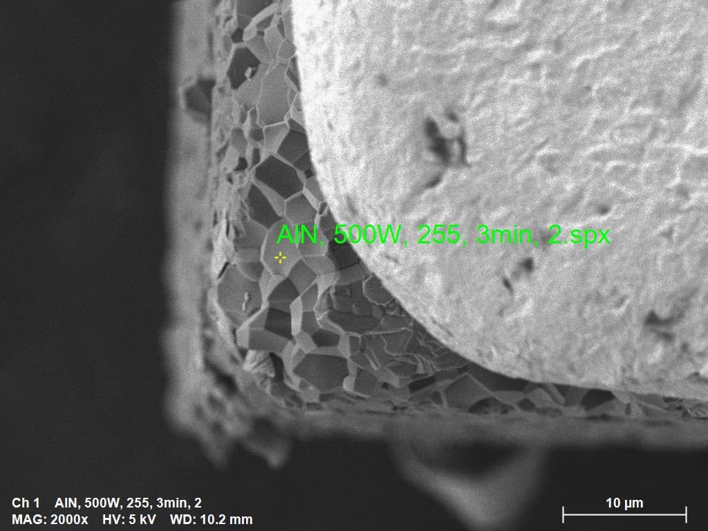
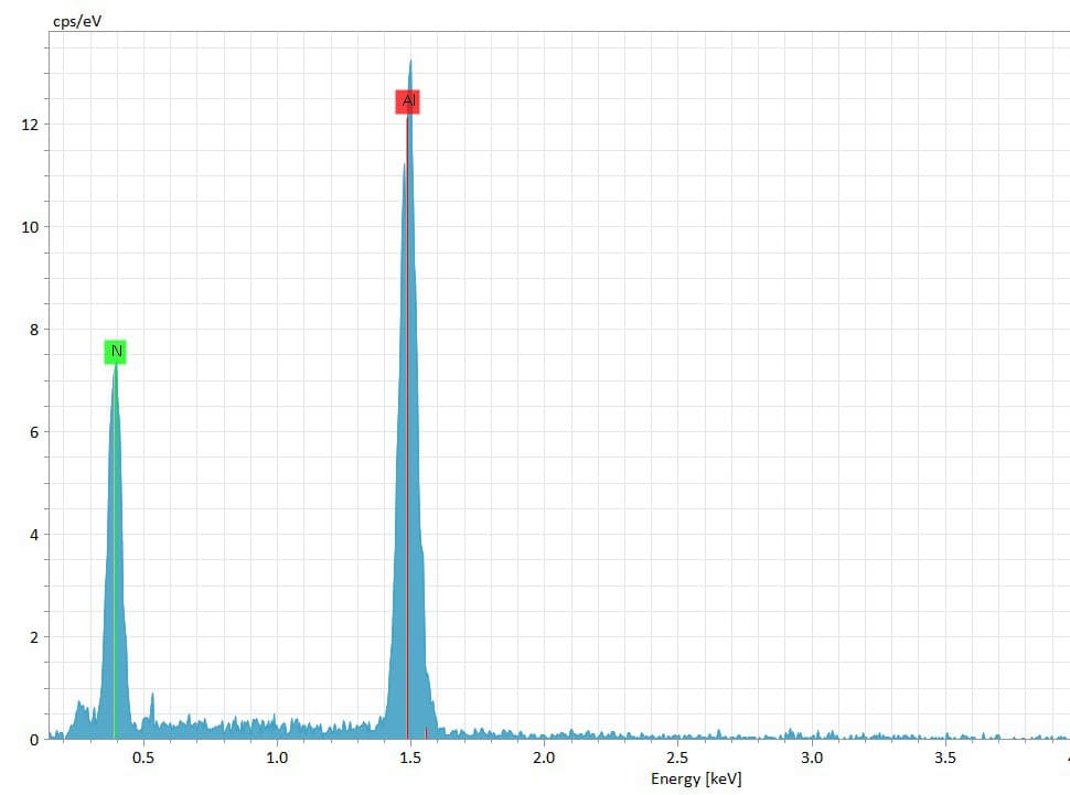
ALN submounts are polycrystalline ceramics. Phonons scatter at grain boundaries, which limits bulk thermal conductivity to 170–210 W/m·K — still 6–8× better than alumina, with excellent CTE match to InP and GaAs laser diodes.
Manufacturing processes
DPC — Direct Plated Copper
Sputter-deposit Cu on ceramic, then build up with electroplating. Delivers the highest patterning resolution (<50 µm) for fine-pitch submounts and densely interconnected photonic layouts.
AMB — Active Metal Brazing
Bond thick copper foil to ALN or SiC using active-metal braze paste under controlled atmosphere. Optimum for high-power modules where current-carrying capacity and thermal cycling life matter most.
DCB — Direct Copper Bonding
Diffusion-bond copper to Al₂O₃ or ALN using a Cu₂O eutectic process. No filler material needed — ideal for power electronics requiring outstanding thermal fatigue resistance.
HTCC — High-Temperature Co-fired Ceramic
Multilayer ceramic co-fired at >1500°C with W/Mo metallization. Used for hermetic SMD packages, TO-replacements, and multi-pin signal housings in defense and telecom.
Standard submount metallizations
| Stack | Thickness | Best for | Notes |
|---|---|---|---|
| Ti/Pt/Au | 1000Å / 1500Å / 5000Å | Universal — wire bond & die attach | Best all-round choice; Pt barrier prevents Au–Ti interdiffusion |
| Ti/Ni/Au | 1000Å / 1500Å / 10000Å min. | Solder die attach, high Au thickness | Ni diffusion barrier active above 350°C — verify reflow profile |
| Au/Sn (80/20) | 3–5 µm | Laser diode die attach preform replacement | Eliminates solder preform handling; avoids rollup at edge pads |
| Ti/TiW/Au | Custom | High-reliability hermetic applications | TiW diffusion barrier; suitable for −65°C to +150°C cycling |
Design tolerances
Three tiers available depending on your application. Contact us to confirm which tier applies to your design.
| Specification | Typical | Select | Critical |
|---|---|---|---|
| Au/Sn pad placement accuracy | ±0.0005" (±12.7 µm) | ±0.0003" (±7.6 µm) | On request |
| Minimum line / space | 50 µm | 25 µm | On request |
| Edge gap (edge-mount laser) | 10 µm | 5 µm | On request |
| Au/Sn solder thickness | 4–6 µm sputtered | 4–7 µm plated | ±2 µm tolerance |
| Substrate thickness tolerance | ±10% | ±5% | ±2% |
| Circuit dimensional tolerance | ±0.002" (50.8 µm) | ±0.001" (25.4 µm) | ±0.0005" (12.7 µm) |
| Front-to-back registration | ±0.001" (25.4 µm) | ±0.0005" (12.7 µm) | On request |
Reliability & hermeticity
Leak rate
≤1.0×10⁻³ Pa·cm³/s
all hermetic packages
Dielectric withstanding
≥500 V AC
between pin and housing
Insulation resistance
≥10,000 MΩ
100 V DC, 25°C
Operating temperature
−65°C to +150°C
qualified range
Thermal cycling
1000 cycles min.
per MIL-STD-810 profile
Marking permanence
MIL-M-13231C
lot traceability
Technical articles
Practical guides and research notes for engineers — including SEM and EDS data from FerraLink ALN and single-crystal SiC material lots.
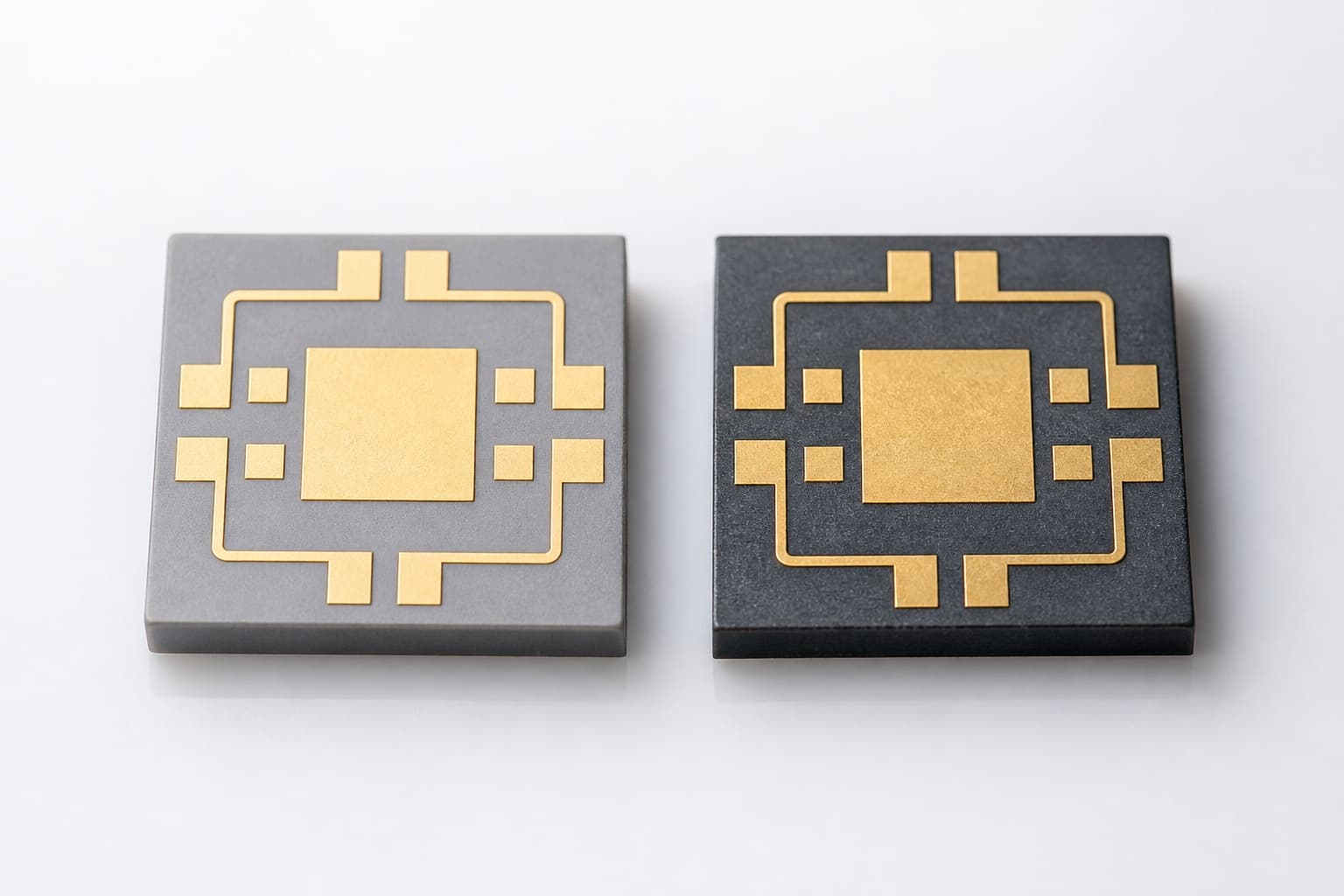
ALN vs SiC Submounts: Thermal Conductivity, CTE, and Cost Comparison
Use polycrystalline ALN (170–210 W/m·K) below ~100 W/cm² for InP/GaAs CTE match; choose single-crystal SiC (350–400 W/m·K) for pulsed lidar, multi-watt bars, and tight Tj margin. Material comparison with decision numbers.
AuSn Pre-deposited Submounts: Why They Improve Assembly Yield
How pre-deposited Au/Sn 80/20 on DPC ALN submounts eliminates preform handling, targets voiding below 2%, and cuts attach cycle time — reflow profile, vs preform economics, and an expandable literature review for laser packaging engineers.
How to Read an EDS Spectrum for Ceramic Submount Incoming Inspection
Energy-dispersive X-ray spectroscopy confirms ALN and SiC composition at receiving inspection. Example spectra from FerraLink material lots with interpretation guidance.
What Is a 14-Pin Butterfly Package?
AuSn Preform vs Pre-Deposited Submount: Decision Tree
FMCW Phase Noise and Junction Temperature Stability
CVD Diamond Submounts: When Single-Crystal SiC Is Not Enough
DPC vs AMB vs DCB on Laser Submounts: Metallization Process Guide
GaN RF Power Module Submount Selection: SiC vs ALN vs Cu-Mo-Cu
Hermetic Packaging for LiDAR Applications
Optical Window Selection for Hermetic Laser Packages
How to Reduce Laser Packaging Costs Without Compromising Hermeticity
Steady-State Thermal Path for CW Laser Diodes: Junction to Heat Sink
Thermal Path Design for Pulsed LiDAR Emitters: Junction to Heat Sink
Transient Thermal and Duty Cycle for LiDAR and Radar Emitters
Void Inspection for AuSn Die Attach: X-Ray Criteria and Reliability
What Is an AlN Submount?
What Is a Laser Diode Submount? Types, Materials, and Selection Guide
What Is a SiC Submount?
What Is a TO-46 Package?
Resources
Datasheets, design guides, and application notes are available on request. Tell us which product you are evaluating and we will send the relevant documents directly.
A technology leader needed hermetic seal packaging for advanced semiconductor applications with tight reliability and timeline requirements. FerraLink delivered custom packaging with unmatched reliability and precision, plus exceptional support throughout the project. The result: a qualified solution that met their performance and program goals on schedule.
Request full case study →Datasheets & application notes by product line
ALN & SiC Submounts
- Datasheet: ALN submount standard sizes and metallization optionsPDF on request
- Design guide: AuSn solder pad layout and placement tolerancesPDF on request
- Application note: CTE matching for GaAs, InP, and Si devicesPDF on request
TO Headers
- Datasheet: TO18 / TO46 / TO56 / TO60 outline dimensionsPDF on request
- Application note: optical window selection (sapphire, AR coat, ball lens)PDF on request
- Design guide: pin count and glass-to-metal seal optionsPDF on request
Hermetic Packages
- Datasheet: butterfly / TOSA / ROSA packages (25G, 100G)PDF on request
- Datasheet: HTCC ceramic SMD and multi-pin packagesPDF on request
- Test report: leak rate, dielectric withstanding, thermal cyclingPDF on request
Optical Transceivers
- Datasheet: SFP / SFP+ / QSFP form factorsPDF on request
- Application note: wavelength selection (850 nm, 1310 nm, 1550 nm)PDF on request
- Qualification summary: industrial and harsh-environment variantsPDF on request
Design guidelines
General design rules
PDFMinimum line/space, via rules, substrate thickness tolerances, and metallization stack options for ALN and SiC.
Thermal performance guide
PDFHow to select substrate material and thickness for your power density and junction temperature target.
CAD data guidelines
PDFFile formats, layer naming, and annotation requirements. Design files accepted in DXF, DWG, or Gerber.
Design for manufacturability
PDFCovers solder pad geometry, pullback rules, AuSn reflow profiles, and assembly best practices.
Company
Our story
FerraLink is a global thermal and hermetic packaging partner for optical, datacom, lidar, RF, and high-power electronics programs. We combine materials engineering, qualified manufacturing partnerships, and clear documentation so teams worldwide can source submounts, TO headers, 14-pin butterfly modules, and cavity packages through one accountable contact.
We own specifications from substrate metallization through package outline — then source production through manufacturing partners that maintain ISO 9001, IATF 16949, and ISO 14001 audited quality systems. Every supplier passes our qualification review before joining the supply chain; each shipment includes certificates of conformance and full lot traceability.
Our focus is thermal performance, hermetic integrity, and engineering outcomes that scale from first prototype to production — not racing to the lowest line-item quote without qualification data behind it.
Team
Leadership
Founder and leadership with deep experience in materials, packaging, and manufacturing for high-reliability applications.
Engineering
Technical team specializing in substrate selection, hermetic sealing, optical packaging, and thermal design — so you work with people who speak your language.
Operations
Manufacturing and supply chain focused on quality, turnaround, and consistency from prototype to production.
Supplier quality systems
Every manufacturing partner in the FerraLink supply chain maintains ISO 9001, IATF 16949, and ISO 14001 audited quality systems — verified before they join our network. Your quote identifies the producing site and the documentation included with shipment.
FerraLink gives you precision submounts, hermetic packaging, and reliable connectivity—with materials expertise and engineering partnership—so you can ship optical and RF systems faster and with confidence.
Schedule a technical walkthrough
Ask a quick question
Have a quick question? Email us at info@ferralink.com.
What happens next?
- •We'll respond within one business day.
- •Next step is typically a short call or email to understand your requirements.
- •We'll recommend options (standard samples or custom at ~2,000 pc MOQ) and provide a quote and lead time.
- •See engineering services and how we work for MOQ and DFM details.
- •No obligation—we're happy to help you scope before you commit.
© 2026 FerraLink. All rights reserved. · Privacy Policy · Terms & Conditions